

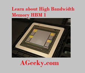
High Bandwidth Memory or HBM 1 memory is a RAM of high performance being used by Advance Micro Devices (AMD) in their latest devices. These devices in which this RAM is being used, also include Hynix. High-end graphics machines and networks need this kind of ram to do their functions properly since this works as a junction between the device and other hardware. HBM 1 is under the use of AMD while HBM 2 NVIDIA. There are some other things such as HBM 2 VS GDDR5, HBM 2 VS GDDR5x. These comparisons are to be made to understand this technology for which we will definitely do some other posts. Right now, let’s move on the working principle of HBM 1 and tell you how does it work?
How does HBM 1 work?
HBM accomplishes higher transmission capacity while utilizing less power as a part of a significantly littler structure element than DDR4 or GDDR5. This is accomplished by stacking up to eight DRAM kicks the bucket, including a discretionary base, pass on with a memory controller, which are interconnected by through-silicon (TSV) and micro bumps. The HBM innovation is comparative on a fundamental level yet inconsistent with the Hybrid Memory Cube interface created by Micron Technology.
HBM memory transport is wide in contrast with other DRAM recollections. For example, DDR4 or GDDR5. An HBM heap of four DRAM bites the dust (4-Hi) has two 128-piece channels per pass on for an aggregate of 8 channels and a width of 1024 bits altogether. A chip with four 4-Hi HBM stacks would along these lines have a memory transport with a width of 4096 bits. In examination, the transport width of GDDR recollections is 32 bits, with 16 channels for a representation card with a 512-piece memory interface
The HBM DRAM is firmly coupled to the host figure bite with an appropriated interface. The interface is partitioned into autonomous channels. Every channel is totally free of each other. Channels are not as a matter, of course, synchronous to each other. The HBM DRAM utilizes a wide interface engineering to accomplish rapid, low-control operation. The HBM DRAM utilizes differential clock. Charges are enlisted at the rising edge if this technology. Every channel interface keeps up a 128 piece information transport working at DDR information rates.
HBM 1 VS GDDR5:
The improvement of High Bandwidth Memory started at AMD in 2008 to take care of the issue. This was of steadily expanding power use and a frame element of PC memory. Amongst different things, AMD created strategies to take care of the kick the bucket stacking issues with a group drove by Senior AMD Fellow Bryan Black. Accomplices from the memory business (SK Hynix), interposer industry (UMC) and bundling industry (Amkor Technology and ASE) were gotten to help AMD understand their vision of HBM. High volume fabricating started at a Hynix office in Korea in 2015.
HBM utilizes Trough Silicon VIA (TSV) technology. It is stacking the memory centers on top of each other on the same base kick the bucket. It is stunning that SK Hynix figures out how to make these layered interconnections trough the silicon. It is one thing to peruse research papers about it. However, seeing the completed item is something else. As should be obvious, HBM chips will be altogether littler than GDDR5 and DDR3 chips.
The HBM1 goes about as a heap of eight 2Gb chips. This brings about 16Gb (2GB) per chip, while the second era HBM duplicates the thickness to 32Gb (4GB) per chip. Also, with 4-Hi HBM2 modules or even 64Gb 8GB with 8-Hi HBM2 memory. This is the way NVIDIA will have the capacity to get 32GB with four chips on Pascal.
So, this was the latest tech info on HBM 1. We will try to bring you more on this one in future. Leave us your feedback about it and stay tuned to our website for more.